How to Create a PCB Layout
The base of the PCB is responsible for holding several components that aid in the functioning of any device. Designers place elements on the board in a particular way for possible wiring. Rules are provided for both the laying and wiring process and must be followed to the latter. Check out PCB layout rules for more information about them. All the layering and routing are a fraction of the PCB layout designing procedure. We discuss the complete PCB layout design process below.
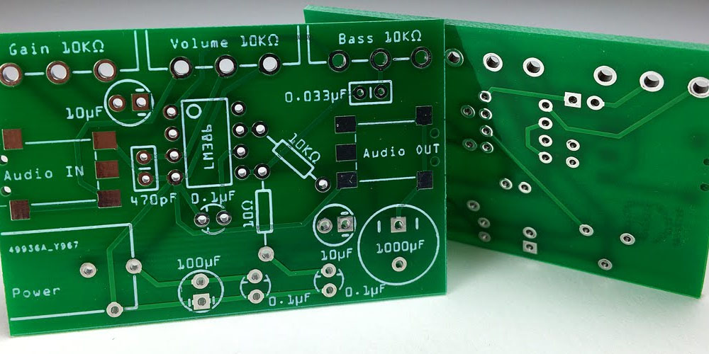
PCB Layout Design Process
The PCB layout design influences how the circuit function. A good design results in a reliable and effective circuit built within the required specifications. The steps for the development process include;
1. Developing a concept
This is a very significant step as it guides the rest of the process. The concept refers to the reason behind the development of the PCB. It involves the PCB application or area of use, its connectivity, quality, size, placement on the electronic device, and other essential factors. PCBs are built differently depending on where they will be used and in which environment. The manufacturer will therefore design them to fit the different temperature ranges. When creating the concept, determine the temperature range limits that the PCB should function within.
2. Creating a virtual circuit drawing
This step is also known as the schematic drawing step. The diagram is not drawn to scale, but it’s a representation of the actual product. Despite the small size, it holds information about the real object, such as its name and hose of the components connected to it, its ratings, values, and how it is meant to function. Recording all elements helps the designer know the materials needed to facilitate the process and also the cost of each. You can also budget for the entire process and proceed with it comfortably.
3. Developing a board-level block
The board-level block is usually a drawing drawn to scale to mimic the final PCB. The designer ensures the proper measurements are made to guide the manufacturer on the scale to use. Sections are then made on the board’s base, and markings are created to indicate the location of every element. The sectioning is done based on how the components connect and work with each other. This process helps minimize the tracing time, making the PCB more efficient.
4. Organizing elements on the board
After the sectioning, the components are now placed on the board as per the markings. In certain instances, all elements are positioned immediately but placed during different times in others. This gives room for refining, evaluation, and the surety that the positions are perfect.
5. Wiring
Also known as routing, it goes hand in hand with the placement of the components. Once every element is secured on the board, the manufacturer does the wiring to complete the circuit and enable the flow of current.
6. Testing the PCB
Testing is essential for ruling out any errors and ensuring the PCB functions as desired. Any product that passes this test is safe for use and can be introduced into the market. However, those that fail must be refined or designed again to make them viable for use.
Conclusion
Designing a PCB layout is something you’d want to focus on and follow the necessary rules. A poor design will cause weak signals and general electric problems, which affect the device. Proper designing prevents such issues and creates something usable, efficient, and convenient.